Getting the Timing Right in Low Power Precision Signal Chain Applications—Part 2
The second article in this series explains timing factors and solutions for reducing power while maintaining precision in low-power systems, as required for measurement and monitoring applications.
This article is published by EEPower as part of an exclusive digital content partnership with Bodo’s Power Systems.
The second article in this series explains timing factors and solutions for reducing power while maintaining precision in low-power systems, as required for measurement and monitoring applications. It explains the factors influencing timing when the ADC of choice is a successive approximation register (SAR) ADC and explores signal chain considerations in analog front-end timing, ADC timing, and digital interface timing. For sigma-delta (∑-Δ) architectures, the timing considerations differ, as shown in Part 1.
Analog Front-End Timing Considerations
The three blocks in Figure 1 can be viewed independently, starting with the analog front end (AFE). The type of signal chain will change the AFE, but some common aspects apply to most circuits.
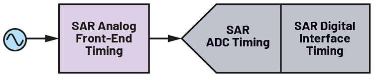
Figure 1. AFE timing considerations with a multiplexed SAR ADC. Image used courtesy of Bodo’s Power Systems [PDF]
Figure 2 shows the AD4696 SAR ADC, the external amplifier, and a low-pass filter comprising the AFE. The AD4696 is a 16-bit, 1 MSPS multiplexed SAR ADC with Easy Drive features. While external amplifiers and circuitry are required to interface with external sensors, Easy Drive features such as analog input high-Z mode and reference input high-Z mode reduce the analog input and reference drive requirements. In higher-power applications, the SAR ADC’s antialiasing filter design needs to be aggressive, but for sampling lower bandwidth signals, typical of low-power applications, the filter design is less demanding. The benefit of a sigma-delta architecture is that we can rely on the digital filter to determine frequency response and use the external antialiasing filter to filter at the modulator frequency. In the absence of oversampling and the inherent filtering qualities, an external analog low-pass filter is required to prevent any higher frequency signals present above the sample rate aliasing into the passband. The low-pass filter also reduces wideband noise from the analog front-end circuitry, reduces the nonlinear voltage kickbacks that occur at the analog inputs, and protects the analog inputs from overvoltage events. The same principle applies to the timing considerations.
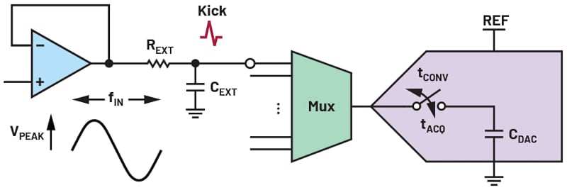
Figure 2. The AD4696 SAR ADC has an external kickback RC filter and a driver amplifier. Image used courtesy of Bodo’s Power Systems [PDF]
While sampling, the SAR ADCs incorporate a sample-and-hold mechanism, a switch, and a capacitor that captures the input signal until a conversion is gathered.
The design of the amplifier stage is a two-step process. The first step is to select the signal conditioning amplifier and external antialiasing stage. The next step is to choose an external driver amplifier (with a bandwidth dictated by the gain; remember there is power vs. bandwidth trade-off) to buffer the signal conditioning antialiasing filters output and drive the ADC input. The next step is to design the kickback filter, taking the total capacitance CEXT + CDAC as the total capacitance of our filter.
Multiplexed SAR ADCs suffer from the issue of kickback when switching between analog input channels. Each time the switch is closed, the internal capacitor voltage (CDAC) may differ from the voltage previously stored on the sampling capacitor (CEXT). A voltage glitch occurs when these switches close due to the difference. The energy will be shared, and the voltage measured between the capacitor terminals will be halved. The CEXT and CDAC values will impact filter designs and must be considered when designing a circuit.
The AD4696 contains an analog input high-Z mode. This significantly reduces the magnitude of the voltage kickback, as seen in Figure 3. The analog input high-Z mode also reduces performance degradation caused by series resistance between the front-end amplifiers and the AD4696 analog inputs, which allows the resistor in the external RC filter to be larger compared to traditional multiplexed SAR ADCs. Using larger REXT with smaller CEXT alleviates amplifier stability concerns without significantly impacting distortion performance, although CEXT = 500 pF minimum is recommended if an internal overvoltage protection clamp is enabled to avoid stability issues. Figure 3 shows that we can sample the required signal quicker, speeding up our system timing.
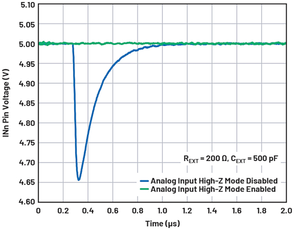
Figure 3. High-Z mode’s impact on kickback. Image used courtesy of Bodo’s Power Systems [PDF]
ADC Timing Considerations
The chosen ADC will depend on what is important in your system. Numerous articles touch on which is a better fit for performance and compare SAR and sigma-deltas technology. In the low-power space, there is plenty of overlap between SAR and sigma-deltas measuring similar signals. One clear thing: SAR timing is more straightforward to understand.
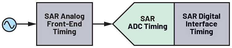
Figure 4. The AFE SAR timing considerations. Image used courtesy of Bodo’s Power Systems [PDF]
SAR ADCs sample the input at a point in time and consist of acquisition and conversion phases. In the acquisition phase, the sample-and-hold network or the internal capacitive network is charged (Figure 2). The capacitor array is switched to a comparator network in the conversion phase. A weighting on the DAC is modified until a code corresponding to the analog input is reached.
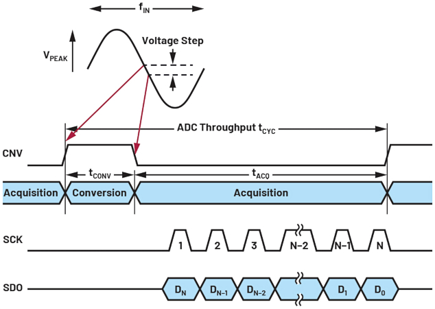
Figure 5. A typical SAR ADC timing. Image used courtesy of Bodo’s Power Systems [PDF]
The maximum conversion time is specified in the data sheet and is 415 ns for the AD4696. The minimum conversion time to acquire the signal is 1715 ns, the acquisition time for the AD4696 while operating at 500 kSPS. The time between conversions is the throughput rate.
Regarding timing, the main trade-off to the SAR ADCs is the power consumption vs. the ADC sample rate. SAR ADCs have the advantage of having a direct linear relationship between the sample rate and supply current, which means it can scale depending on the bandwidth of the signal of interest. The internal ADC core powers down between conversions, so when operating at lower sample rates, 10 kSPS, for example, the AD4696 typically consumes 0.17 mW vs. 8 mW at 1 MSPS, making the devices suitable for battery-powered applications at lower sample rates.
Figure 6 shows the VDD current. If we reduce the sample rate of the AD4696 to work in the sub 100 kSPS range vs. at 500 kSPS, our IDD current drops from almost 2.5 mA to 0.5 mA. If we reduce the current to 10 kSPS, our typical IDD current reduces to 42 µA. The rate of increase in current is linear. All digital and analog supply currents scale similarly linearly, making the SAR ADC an attractive proposition for measuring DC-to-AC signals using the same part.

Figure 6. VDD current vs. sample rate. Image used courtesy of Bodo’s Power Systems [PDF]
Digital Interface Timing Considerations
Several features associated with the AD4696 would not be traditionally associated with SAR ADCs that can help low-power signal chain designers achieve additional power savings but with timing implications.
Figure 7. SAR digital interface timing considerations. Image used courtesy of Bodo’s Power Systems [PDF]
A SAR ADC’s throughput rate, in comparison to the sigma-delta architecture, is easier to calculate as filter latency does not need to be considered:
\[Throughput,Rate(SPS)=\frac{1}{t_{CYC}}\div CHs\,\,\,\,\,(1)\]
CHs = the number of channels enabled.
The cycle time is the time between CNV rising edge transitions and consists of a combination of the acquisition and conversion phases, but there can be overlap. The ADC can acquire a signal while the conversion phase is still occurring. The time between samples on a SAR ADC can be described as cycle time tCYC or sample rate time tSR.
tCONVERT = conversion time tACQ = acquisition time
tCYC = tSR = inverse of the sampling frequency, the time between samples
The sample instant of when the conversion takes place is controlled by the CNV signal rising edge. In most modes, this is provided by an external signal. The AD4696 also has an on-chip autocycle mode that can generate the convert start signal internally. This signal kickstarts the conversion. Several sequencer modes are available on the AD4696, allowing the user to choose the order and configuration of conversions in a predefined fashion or control the next channel in the sequence on the fly without interrupting conversions.
The digital host must read back the data before the start of the next conversion. With higher speed signals, the SCK frequency must be fast enough to read back the data from the AD4696 SPI before the next CNV rising edge (or internal convert start signal when in autocycle mode). Faster sample rates require faster SCK frequencies because the time between conversions is shorter.
The minimum required SCK frequency is a function of the sample rate, the length of the SPI frame (in bits), and the serial data output mode in use. Conversion results for a given sample are available until the start of the next conversion phase. The SCK frequency must, therefore, be fast enough to read the data from the AD4696 SPI before the following CNV rising edge (or internal convert start signal when autocycle mode is enabled).
Multiple SDO Digital Outputs
The AD4696 family also includes dual-SDO and quad-SDO modes. ADC results are shifted out on SDO and additional GPIO pins in parallel in these modes. These modes significantly reduce the required SCK frequency for a given sample rate by doubling or quadrupling the number of bits output on the SPI per SCK period. This reduces the requirement on the microcontroller, which reduces the required clock from 32 MHz SPI clock to 16 MHz SPI clock when converting at 1 MSPS.
The number of SCK periods required per conversion mode frame (NSCK) is a function of the number of bits per frame (NBITS) and the number of serial data outputs (NSDO):
\[N_{SCK}=\frac{N_{BITS}}{N_{SDO}}\,\,\,\,\,(2)\]
Where NSDO is 1 for single-SDO mode, 2 for dual-SDO mode, and 4 for quad-SDO mode.
The start of the conversion mode SPI frame must not occur before the tCONVERT time has elapsed and must be completed early enough to adhere to the minimum tSCKCNV specification. The amount of time given to complete an SPI frame in conversion mode (tFRAME) is calculated as follows:
tFRAME = tCYC – tCONVERT_max – tSCKCNV
Where tCYC is the sample period, tCONVERT_max is the maximum, tCONVERT is the specification, and tSCKCNV is the SCK to CNV rising edge delay specification.
The fSCK is a function of tFRAME and NSCK.
\[f_{SCK}>\frac{N_{SCK}}{t_{FRAME}}\,\,\,\,\,(3)\]
The AD4696 data sheet includes a table with examples of minimum SCLK frequencies vs. several sample rates.
Autocycle Mode
For voltage or current level monitoring applications, traditionally, SAR ADCs require a host controller to issue a continuous convert signal for conversions. The system needs to examine the data for thresholds and make decisions based on these levels. This is not power efficient because the host must continually convert. The AD4696 can be configured to convert autonomously on a user-programmed channel sequence.
Autocycle mode is a great mode to use for monitoring analog inputs. There are several options for the conversion period ranging from 10 µs (100 kSPS sample rate) to 800 µs (1.25 kSPS sample rate). This mode can be used with threshold and hysteresis detection alerts configurable per channel to reduce overhead for the digital host system. In this scenario, the host controller can enter a low power state and only power up when it receives an interrupt from the AD4696 when a level is triggered.
Oversampling
Oversampling and decimation are inherent to sigma-delta architecture. The AD4696 SAR ADC includes an oversampling and decimation engine for further noise reduction. It effectively averages consecutive ADC samples to generate an oversampled result with higher effective resolution and lower noise. The effective number of bits increases by 1 bit every time the oversampling ratio (OSR) is increased by a factor of 4 on the AD4696.
This is especially useful in measuring a slower-moving signal found in a low-power signal chain application, such as temperature, that requires higher precision.
\[t_{SAMPLE}=t_{CYC}\times OSR\,\,\,\,\,(4)\]
Where tSAMPLE = the sample period, tCYC = cycle time (1/sample rate), and OSR = oversampling ratio (a programmable value between 4 and 64).
The trade-off, similar to sigma-delta ADCs, is between performance and speed.
Table 1. SAR Summary
| Topic | Timing Considerations | Low-Power Signal Chain Impact |
| Antialiasing Filter | Delays can exist that impact the first conversion result(s) | Less aggressive filtering is needed compared to higher-speed signal chains |
| High-Z Mode | The kickback time is reduced when switching channels | Power scales with sample rate; less external circuitry |
| Current vs. Sample Rate | Reducing power reduces your sample rate | Reducing your sample rate reduces the power |
| Autocycle Mode | Software configurable internal convert start | The host controller can enter a low-power state |
| Dual-SDO and Quad-SDO | At higher sample rates, readback of all data is not possible with a single SDO | The trade-off between extra circuitry and data speeds |
| Oversampling | The interval between samples increases as the oversampling increases | Increasing OSR improves noise and resolution performance |
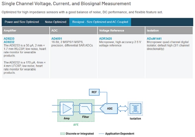
Figure 8. The precision low power signal chains webpage. Image used courtesy of Bodo’s Power Systems [PDF]
Low-Power Precision Platforms
As the trend in energy cost increases globally and we learn about the impact of our energy usage on the natural world, system designers are working to achieve precision with reduced power budgets. It can be difficult to research and find the lowest power components available. Analog Devices is simplifying the design process by taking our lowest-power precision components and providing a one-stop shop with ready-to-go signal chains and circuits that supply system designers with the most up-to-date precision low-power offerings.
Example: Low-Power SAR Signal Chain
Many applications require the measurement of a small signal on top of a large DC offset or common-mode voltage. If a system aims to monitor flow in an industrial environment or make a biopotential measurement, there is overlap in the approach. These signals typically need AC coupling to remove the large offset as well as biasing and gain to maximize the dynamic range of the ADC.
Our low-power precision signal chains suggest which devices to choose for this type of application.

Figure 9. A signal chain example. Image used courtesy of Bodo’s Power Systems [PDF]
In addition, know-how with integrated knowledge (KWIK) circuits provides a more in-depth analysis of circuits and the latest suggestions on up-to-date components.
Flow Signal Chain Example
For example, we want to design a large multi-measurement system that includes flow measurement using the KWIK circuit shown in Figure 10.
A: I want to run ten flow sensors at 1 kSPS. Is the SAR or sigma-delta the better option?
B: What are the AFE timing considerations?
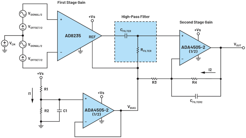
Figure 10. The flow measurement signal chain KWIK circuit. Image used courtesy of Bodo’s Power Systems [PDF]
The best options are the SAR (AD4696), in conjunction with the AD8235 and ADA4505-2 amplifiers needed for signal conditioning. We can run ten channels at 10 kSPS using an external convert signal or auto-cycle mode.
In this case, the response vs. gain of the AD4505-2 amplifier will dictate the BW of the signal under measurement rather than the antialiasing filter response. The high-Z mode will take the pressure off the performance of the input amplifier, enabling designers to choose lower-power amplifiers. The components in Figure 10 are selected for their ultra-low power performance.
Takeaways of Timing in Low-Power Precision Signal Chain Applications
When designing high-resolution, low-power data acquisition systems, it can be difficult to find the lowest-power components available, and precision low-power signal chains act as a starting point for low-power designs. Care must be taken to understand the trade-offs and differences in timing when forming signal chains that incorporate sigma-delta and SAR architectures as their core ADC.
When interfacing with sensors or signals of interest, the analog front-end timing must account for chip-level startup, sensor biasing, external filtering, and component choice. Antialiasing filters are needed with stricter requirements on SAR ADCs because sigma-delta ADCs have inherent sampling associated with their design. On the AFE, sigma-delta ADCs incorporate PGAs while SAR technology like high-Z mode is easing the drive requirements on external amplifier circuitry.
When we consider sigma-delta ADC architecture, oversampling, decimation, and filter latency impact the throughput rate especially while converting on more than one channel. On the other hand, SAR throughput is more straightforward to calculate because of the successive approximation approach, with the added benefit that the slower you sample, the lower the current drawn while converting.
The complexity of the sigma-delta AD4130-8 digital timing has led to the development of ACE software timing tools. These are available to simplify the understanding and aid in calculating the channel throughput rate. The same device has timing features like duty cycling, FIFO, and a standby mode to help conserve battery life. Still, care is necessary to determine the achievable effective resolution when targeting a particular throughput rate.
When examining a SAR ADC like the AD4696, we can sample at higher frequencies. This has advantages but means the digital timeframe, tFRAME, in which you need to read back is smaller, meaning faster SPI clock speeds are required.
This article originally appeared in Bodo’s Power Systems [PDF] magazine.